Induction Heating Techniques for Semiconductor Crystal Growth
 Semiconductors play a pivotal role in the global economy. That may sound like a bold claim, but it’s a basic fact as we move further into the 21st century. Induction heating is a critical tool in semiconductor manufacturing.
Silicon is the most widely used material in semiconductor manufacturing, and induction heating provides an efficient process for developing monocrystals (and, ultimately, semiconductor wafers). Due to silicon’s abundance and cost-effectiveness, it’s a great material for this technology. The silicon semiconductor wafers serve as a substrate for integrated circuits.
When manufacturing monocrystals for semiconductor uses, consider the quality of silicon. Your input material influences the efficiency, speed, and power consumption of the final semiconductor devices. With global demand surging, this is important.
So, for your purposes, how can induction heating play a critical role in growing those crystals?
How to Grow Silicon Monocrystals with Induction Heating
There are two prevailing processes for crystal growth.
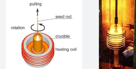
Czochralski (CZ) Process
The CZ process is the predominant method for growing silicon monocrystals.
This process involves melting high-purity silicon in a crucible at temperatures just above its melting point of 1,414°C. A precisely oriented seed crystal is dipped into the molten silicon and slowly withdrawn, with careful rotation and controlled temperature gradients, to generate and grow a cylindrical silicon ingot shaped by the orientation of the seed.
Induction heating ensures uniform heating of the silicon melt, and that’s important because a stable melt and temperature gradient prevents defects in the growing crystal.
The ability to precisely control the power output of the induction heater allows you and your team to fine-tune the temperature within the crucible, enabling the growth of large-diameter silicon crystals with high purity and minimal defects.
Float Zone (FZ) Process
The FZ process is another technique used for growing high-purity silicon crystals, particularly for applications requiring a much more refined final material.
This method avoids potential contamination from crucibles used in the CZ process. When working with this method, induction heating equipment creates a localized molten zone in a rod of polycrystalline silicon without the need for a crucible.
In this method, a rod of polycrystalline silicon is passed through a narrow, radio-frequency induction-heated zone, which melts a small section of the rod. The molten zone is slowly moved along the length of the rod, recrystallizing it into a single crystal behind the zone. The result is a highly pure silicon crystal.
Since the silicon does not come into contact with any container, there is significantly less risk of introducing impurities into the process. As such, the FZ process is efficient when pursuing certain semiconductor applications. Induction heating units can be adjusted to modify the size and temperature of the molten zone, allowing for better control over the crystal growth rate and orientation. This adaptability is essential for tailoring the crystal properties to specific requirements.
Challenges in Growing Silicon Monocrystals
While these processes have flourished in manufacturing settings for decades, the actual technology and workflow continues to evolve. Growing silicon monocrystals is a complex and delicate process that requires precise control over numerous parameters, including temperature, crystal pulling speed, and ambient atmosphere.
Any fluctuations can introduce defects into the crystal, which can degrade the performance of the semiconductor devices made from the wafers. Advanced monitoring and control technologies are continuously being developed to improve the quality and yield of silicon monocrystals.
As far as induction heating equipment goes, you must know that crystal growth requires a very hands-on approach:
- The design of the induction coil and the electromagnetic field it generates must be optimized for each process to ensure uniform heating and minimal disruption to the crystal growth.
- The frequency of the power supply to the induction heater affects the penetration depth of the heating in the material. Adjusting the frequency can help in controlling the heating profile for different stages of the crystal growth process.
- Effective thermal management is crucial, especially in the CZ process, to control the temperature gradient and cooling rates, which influence the crystal’s structural integrity.
Future Directions
As the technology behind semiconductor devices continues to evolve, there is an ongoing demand for silicon monocrystals with even higher purity and defect-free structures.
Innovations in crystal growth techniques, such as improved induction heating technologies and advanced process control systems, are essential for meeting the stringent requirements of next-generation semiconductor devices. Research is also focusing on alternative materials and methods for semiconductor manufacturing, which could complement or replace silicon in certain applications.
The ability to produce high-quality silicon monocrystals directly impacts the advancement of semiconductor technology, driving ongoing research and technological developments in this critical field.
Induction heating’s precise control, efficiency, and ability to provide uniform, contaminant-free heating environments are indispensable for the production of high-quality silicon monocrystals in both the CZ and FZ processes. These characteristics make induction heating a cornerstone technology in the field of semiconductor manufacturing.
Research
Research is an important backdrop in understanding the impact of induction heating applications. We’ve gathered a few studies that can provide greater depth on the topic of crystal growth for semiconductor manufacturing.
Three-dimensional CZ silicon melt flow under induction heating
Model experiments for Czochralski crystal growth processes using inductive and resistive heating